Printed Circuit Board
2011.01.25
George Hines, Mechanical Engineering Director
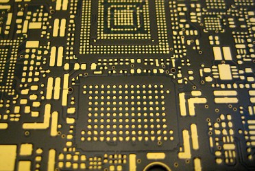
Here is the first PCB (printed circuit board) layout for the Æ+Y phone, before being populated with all the individual electronic components. It’s a process that is always taken for granted because it is internal to the phone, but has always fascinated me as an engineer, as you can imagine a number of other images when you look at the picture — maybe a skyline or a game of Pac-Man!